Русский
английский
ПОДДЕРЖКА КЛИЕНТОВ И ПРОДАЖИ
[tracy@cady-ic.com]
Переключить навигацию
Категории
Домой
О нас
Производители
CHIP
Новости
Новая компания
Отраслевые новости
Гарантия качества
Политика качества
Соответствие RoHS
Качество и соответствие требованиям
Применения
Домашнее приложение
Промышленное применение
Решения для быстрой зарядки постоянного тока
Рельсовая тяговая передача электроэнергии
RFQ/Котировка
Свяжитесь с нами
Дом
>
Производители
>
CHIP
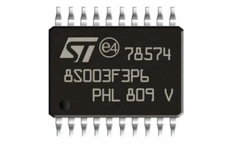
STM8S003F3P6 Description STM8S003F3P6 is a microcontroller unit (MCU) developed by STMicroelectronics. It is a highly integrated device that combines the processing power of a central processing unit (CPU) with memory,
ЗАПРОС
ПРЕДЫДУЩИЙ:
Следующий:
ИНФОРМАЦИЯ
WhatsApp:
Email:
Содержание:
Captcha:
Отправить
Сбросить
СОПУТСВУЮЩИЕ ПРОДУКТЫ
Категории
CHIP
ПОСЛЕДНИЕ НОВОСТИ
Расширенная семья переключател...
Fuji Electric 7-го поколения I...
Повышайте эффективность ваших ...
More Power, Less Space
СВЯЖИТЕСЬ С НАМИ
Контакт: tracy
Слева свяжитесь с нами
Share
Call
Menu
Top